


Information
First-Time Exhibition at SEMICON China 2025 (March 26–28)
March 19th,2025 exhibition
Takano Co., Ltd. (Headquarter: Nagano Prefecture; CEO: Jun Takano) will make its debut at "SEMICON China 2025," the world's fastest growing microelectronics market exhibition, in Shanghai, China in March 2025. TAKANO will highlight highly precision semiconductor inspection equipment and introduce "PSL deposited Wafer," to support better in semiconductor manufacturing quality control.
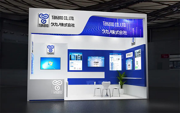
SEMICON China 2025 exhibition booth image
Admission is free with pre-registration. Please apply through the visitor pre-registration site.
▽Exhibition Invitation Ticket Application (Free)
https://semi.expotec.com.cn/
SEMICON China 2025 exhibition booth image
Background of the Exhibition
Takano Co., Ltd. has been developing, manufacturing, and selling products for semiconductor inspection and other equipment with own optical inspection technology, serving the industry more than 30 years and over 1000 products delivered to mostly domestic and some overseas customers. In recent years, there is no doubt that China became fastest growing region and the role of our technology should plays to serve you to build more robust foundation and growth.
This year, we are given first opportunity to participate in "SEMICON China 2025" to introduce ourselves with inspection equipment and the newly launched service product, PSL deposition wafer. This service is expected to contribute robust and stable quality control in particularly particle control processes.
Please stop by the Takano booth and see by your own eyes, then talk to us what you think.
SEMICON China 2025 Outline
| Dates: | March 26 (Wed) to March 28 (Fri), 2025 |
| Venue: | Shanghai New International Expo Center (SNIEC) |
| Organizer: | SEMI China |
| Booth Number: | T2225 |
| Official Website: | https://www.semiconchina.org/ |
Admission is free with pre-registration. Please apply through the visitor pre-registration site.
▽Exhibition Invitation Ticket Application (Free)
https://semi.expotec.com.cn/