製品情報
Product Information
Product Information
Visual Inspection System Comming Soon
One system, All solution
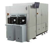
Takano develops and manufactures high performance Inspection and Metrology system and delivers high solution supporting the Semiconductor industry from R&D to the HVM (High Volume Manufacturing) environment, provided combination inspection system of 2D and 3D capabilities on the same platform.
This system has high performance inspection capabilities of bump CD measurement, General surface inspection, full wafer bump 3D inspection and metrology and RDL inspection and Metrology.
This system provides an automated inspection solution from high bump application of FPGA, CPU and GPU to low bumps application of WLP, IC drivers, RF filter and MEMS.
Application
- FoWLP (Fan out Wafer Level Package)
- FoPLP (Fan out Panel Level Package)
- TSV (Through Silicon Via)
- CIS (CMOS Image Sensor)
- MEMS (Micro Electro Mechanical Systems)
- RF filter
Product Specification
2D Inspection| Inspection Capabilities | Detect 1.0 μm RDL pattern at High throughput |
|---|---|
| Resolution | 0.5μm~ |
2D metrology
| Object types | Bump, RDL, Pad |
|---|---|
| Inspection capability | Bump diameter, line width, line length, placement deviation |
| Accuracy | 0.1 μm |
| Repeatability | 0.2 μm at 3σ |
| UPH | 30 wafers (12inch) |
| Bump types | Solder, copper pillar, micro bumps |
|---|---|
| Inspection Capabilities | Bump height, co planarity |
| Height Accuracy | 0.2 μm |
| Height Repeatability | 0.2 μm at 3σ |
| Measurement Range | ~ 60 μm |
| UPH | 7 wafers (12inch), 20 wafers (2019~) |
Contact Us
Please contact us from the form below.