


Information
Exhibition at "SEMICON Taiwan 2025" from September 10 to 12
August 27th,2025 exhibition
We will exhibit at “SEMICON Taiwan 2025,” held from Wednesday, September 10 to Friday, September 12, 2025, at Taipei Nangang Exhibition Center, Halls 1 and 2 (Tainex), Taiwan.
This time, we will exhibit semiconductor inspection systems and new technologies for device manufacturers, foundries, equipment manufacturers, and material manufacturers. At Takano, we cover a wide range of inspection from optical to laser inspection. Please be sure to stop by our booth.
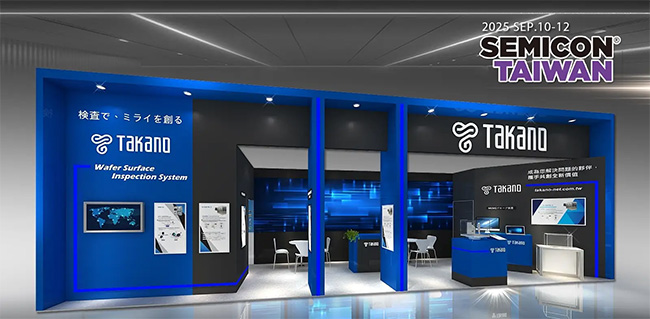
SEMICON Taiwan 2025 Booth Image
SEMICON Taiwan 2025 Event Overview
| Dates: | September 10 (Wed) – 12 (Fri), 2025 |
| Hours: | 10:00–17:00 (until 16:00 on the final day) (local time) |
| Venue: | Taipei Nangang Exhibition Center, Halls 1 & 2 (Tainex), Taiwan |
| Booth No.: | N1383 |
| Official Website: | https://www.semicontaiwan.org/ ▽ Visitor pre-registration here https://registration.semicontaiwan.org/visitor/index |
Exhibits
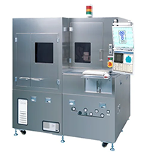
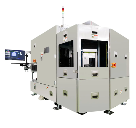
Wafer Surface Inspection System – WM Series
This is an essential inspection system for semiconductor device manufacturing, material development, and equipment management.
It can detect particles (foreign matter) at the nanometer level and is widely used both in Japan and overseas. A semiconductor laser is used as the light source, helping reduce running costs.
WM-7R+ and WM-10R+ have obtained international safety certifications. These are the latest models with a renewed exterior design. While maintaining performance equivalent to previous models, the new design enhances brand consistency and appeal.
▼ For details, click here
https://www.takano-kensa.com/kensa/products/semiconductor/wm/
-
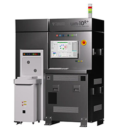
WM Series: WM-10R+ -
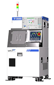
WM Series: WM-7R+
This is an essential inspection system for semiconductor device manufacturing, material development, and equipment management.
It can detect particles (foreign matter) at the nanometer level and is widely used both in Japan and overseas. A semiconductor laser is used as the light source, helping reduce running costs.
WM-7R+ and WM-10R+ have obtained international safety certifications. These are the latest models with a renewed exterior design. While maintaining performance equivalent to previous models, the new design enhances brand consistency and appeal.
▼ For details, click here
https://www.takano-kensa.com/kensa/products/semiconductor/wm/
Inspection System for TGV “ALTAX”
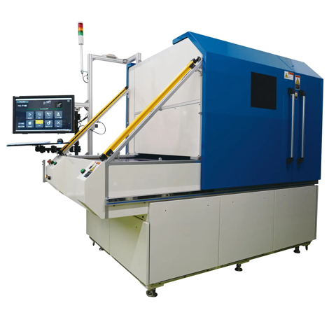
Inspection System for TGV “ALTAX”
This newly developed system enables high-speed inspection of via diameter and position, cavity shape, and the depth of every via after copper filling in the Through Glass Via (TGV) manufacturing process. It measures 510 mm × 515 mm substrates in about 120 seconds (at 6 μm resolution) and supports a wide range from R&D to mass production lines.
▼ For details, click here
https://www.takano-kensa.com/kensa/products/semiconductor/altax/
Micro-Load Displacement Measurement System “TST-001-P” (Under Development)
This is a newly developed system capable of measuring extremely small loads and displacements with high precision. It supports simultaneous measurement of stress, displacement, and resistance, enabling characterization of various samples such as probes, cantilevers, piezoelectric actuators, and membrane materials. Measurement results can be graphed in real time and saved as video, making it widely useful from R&D to quality control. It achieves a resolution of 0.0001 N for stress and 0.1 μm for displacement, contributing to high-precision evaluation in semiconductor manufacturing.
▼ For inquiries regarding this product, please contact us here
https://www.takano-net.co.jp/newtechnology/contact/
Wafer Appearance Inspection System (Vi Series)
This system performs high-precision inspection of wiring patterns, cracks, and foreign object contamination on wafers. Depending on wafer size, device, defect type, and inspection speed, we can propose from five product lineups. 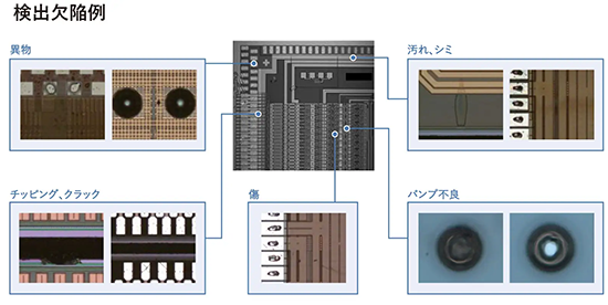
▼ For details, click here
https://www.takano-kensa.com/kensa/products/semiconductor/pattern/
This system performs high-precision inspection of wiring patterns, cracks, and foreign object contamination on wafers. Depending on wafer size, device, defect type, and inspection speed, we can propose from five product lineups.
-
Vi-4207 -
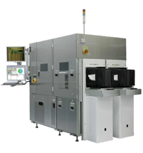
Vi-4307 -
Vi-5301
▼ For details, click here
https://www.takano-kensa.com/kensa/products/semiconductor/pattern/
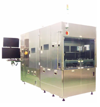
Full-Surface Film Nonuniformity Inspection System (Thinspector)
Full-Surface Film Nonuniformity Inspection System (Thinspector)
Performs high-speed, full-wafer film thickness measurement and nonuniformity inspection in a single scan, enabling comprehensive thickness control without omissions.
▼ For details, click here
https://www.takano-kensa.com/kensa/products/semiconductor/thinspector/
Film Appearance Inspection System – Hawkeyes Series
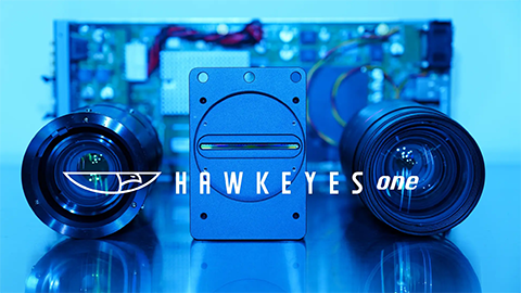
High-Speed Fine Image Inspection System Hawkeyes one
The Hawkeyes series achieves high-speed and high-precision inspection for the high-performance film market (optical, electronic components, battery materials) by adopting in-house cameras, image processing units, and inspection algorithms.
By employing an in-house high-performance camera and a newly developed image processing unit, it achieves industry-leading inspection speeds (according to our research). High-resolution settings are available to detect micro-defects on high-speed production lines. In addition, parallelization of multiple processes enables diverse defect detection.
▼ Product page for High-Speed Fine Image Inspection System Hawkeyes one
https://www.takano-kensa.com/kensa/products/film/one/
Launch of PSL-Particle-Coated Wafer Sales (New Service)
These are PSL (polystyrene latex) particle–coated wafers, essential for the management of semiconductor equipment. PSL particle–coated wafers are used for calibration and evaluation of wafer surface particle inspection systems and play an important role in ensuring detection sensitivity and accuracy.
We can apply PSL particles of various sizes onto wafers according to your needs.
This contributes to foreign-matter control in the manufacturing process, equipment performance maintenance, and improved yield. We invite you to utilize “PSL particle–coated wafers” to help improve the quality of your semiconductor manufacturing processes.
Details will be explained at the Takano booth, so please feel free to consult us about the optimal PSL coating service.