


Products
Bump Height Inspection System
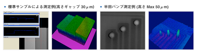
 This system measures the height, diameter, and coplanarity of bumps formed on package substrates such as semiconductor wafers, BGAs, and CSPs at high speed and with high accuracy. The use of an optical system that has been independently improved and a data processing method (Time Delay Scanning) enables high-precision measurement that is not possible with the conventional light-section method.
Features
- High accuracy measurement of bump height and coplanarity 3σ ≤ 1.0µm.
- Inspection time per sample is less than 2 seconds. With our unique processing algorithm and dedicated processing equipment, it is possible to process tens of thousands of high-density bumps at high speed.
- Minimum measurable size is φ30µm.
Specifications
| Substrate size | Wafer: 2inch ~ 12inch Substrate: 20mm×20mm~ |
|---|---|
| Inspection resolution | For height inspection measurement (standard): Horizontal resolution (X, Y) = 5.8 µm, Z = about 0.1 µm |
| Measurement accuracy | Height / coplanarity: 3σ ≤ 1.0µm |
| Measurement Z range | Z = 150µm (can be changed) |
| Inspection tact | ~ 10wafer / h (12inch wafer) |
| Measurement method | Light cutting method + TDS (Time Delay Scanning) method |
| Target bump | Minimum bump diameter: φ30µm / φ60µm ~ (* Depends on base material and bump shape) Minimum bump pitch: about 60μm / 100μm ~ |
| Inspection item | Height, coplanarity, board warpage (Optional) Bump diameter, bump area, bump volume, bump missing / bridge |
Inspection target / use / option
Solder bumps on package substrates such as BGA / CSP, Au bumps on semiconductor wafers.
Contact Us
Please contact us from the form below.