


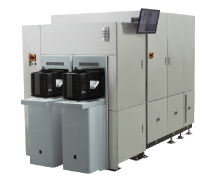
Products
Takano provides customers in semiconductor industry with high reliability solutions, through manufacturing and developing high performance Inspection and Metrology systems.
Product List
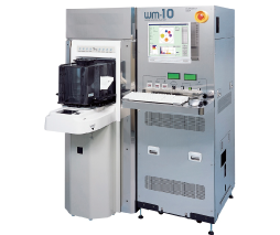
Inspection system that can detect particles on the surface of bare wafer with high sensitivity.
This system is used in various situations for process control.
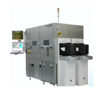
The optical inspection system with high speed and accuracy that can finds wiring patterns,
cracks, and particles and etc.
While conventional commercial spot film thickness measurement systems manage film thickness by measuring only a few points across the wafer, Takano's Thinspector can inspect the entire wafer surface in a single scan.
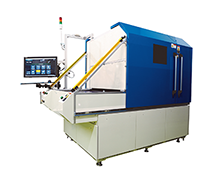
Inspection system that can measure the height, diameter, and coplanarity of bumps formed on
package substrates such as semiconductor wafers, BGAs, and CSPs
at high speed and with high accuracy.
Minimum measurable size is φ30um.
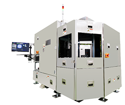
This system measures non-destructive, high-speed measurement of TSV,
which is indispensable for 2.5D and 3D laminated structures,
and trench depth of power semiconductors.
For more information, please contact our maintenance service.
This system has ability to inspect of 2D and 3D capabilities on the same platform.
Contact Us
Please contact us from the form below.