
Flat Panel Display (FPD) High-Precision Inspection System

About High-Precision Inspection System
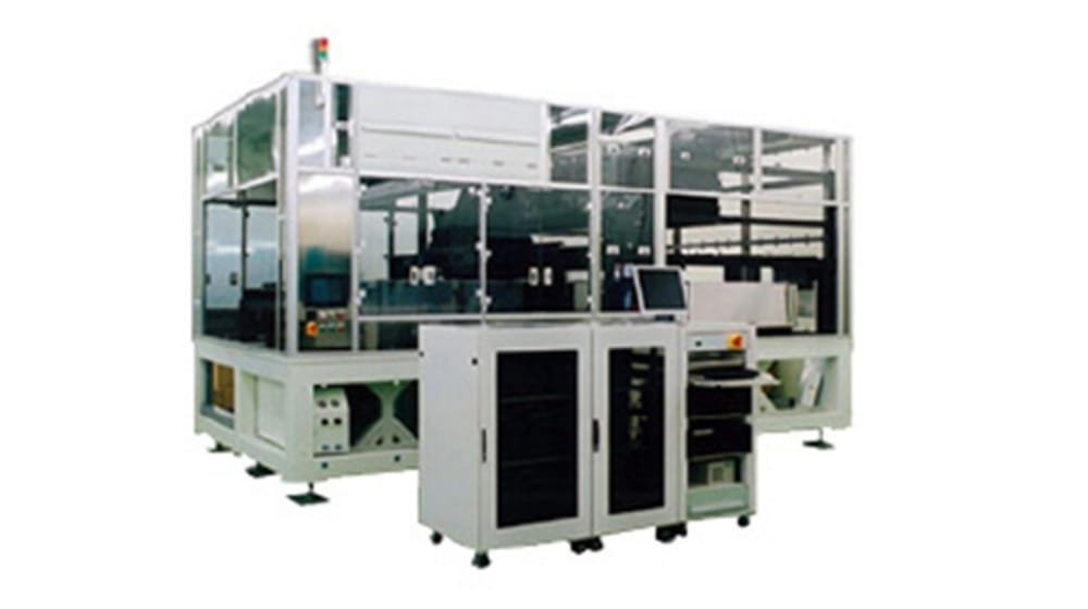
This equipment can inspect micro-patterns in LCDs, OLEDs, touch panel substrates, and other similar products. Image data captured by a line sensor camera equipped with high-resolution lenses and an optimized optical system is processed at high speed by our proprietary image processing unit, allowing for real-time monitoring of substrate conditions.
Inspection Targets
- LCD (CF, TFT)
- OLED Displays
- Touch Panels, etc.
Defect Detection Example
-
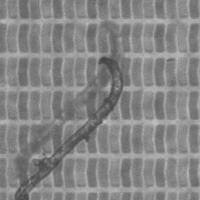
Unpatterned Wafer Surface Inspection System -
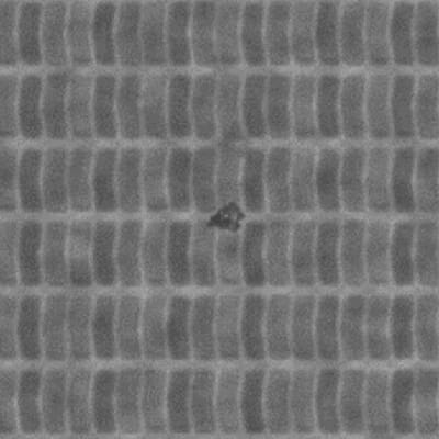
Foreign Material -
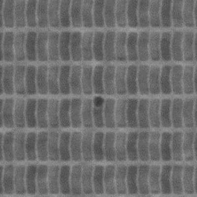
Pinhole
And more.
Features
-

Original algorithm “GFC” enables the detection of minute defects.
-

TAKANO's original high-speed image processing technology combined with high-precision inspection lenses allows for fast and stable inspection.
-

Proven track record up to G10.5 substrates.
Specifications
| Maximum Resolution | 3μm/pixel |
|---|---|
| Camera | In-house Line Sensor Camera (16000 pixels (560MHz) / 7400 pixels (266MHz)) |
| Illumination Method | High-brightness LED illumination / Optical filters tailored to each process |
| Inspection Stage | Free Roller / Air Slider / Linear Motor Stage |
| Review Unit | Zoom microscope, optical magnification x5.0 to x50 / high-speed autofocus unit (Include traceability mode) |
| Defect Detection Capability | 3μm or larger |
| Example Tact Time | 30 sec/sheet (at 5μm detection capability) |
Options
- Stain Inspection Function: Detects low-contrast defects such as stains.
- High-speed Image Transfer Function: Rapidly transfers defect images along with defect information during inspection.