
Patterned Wafer Visual Macro Inspection System (Vi Series)

About the Vi Series
Vi Series delivers high-speed, high-precision inspection of circuit patterns, cracks, foreign particles, and other surface defects. This flexible system accommodates all inspection needs while providing outstanding cost efficiency.


Applications
- Patterned silicon wafers
- Filmed wafers
- Compound wafers
- Transparent wafers
- Glass substrates
- Tape frames
- Thin wafers
Target Markets
- Foundries
- Semiconductor device manufacturers
- RF filters
- R&D, and more.
Defect Detection Example
-
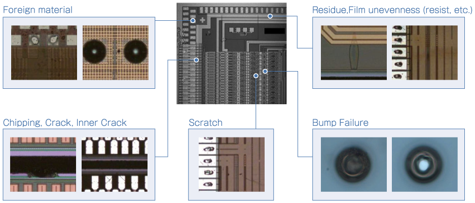
Defect Detection Example
-

High reliability backed by
an extensive installation base -

Detects defects using Takano’s proprietary algorithm
-

Compatible with wafers
and tape frames -

Capable of inspecting inner-cracks after dicing process
Specifications
| Item | Vi-4207 | Vi-4307 | Vi-5301 |
|---|---|---|---|
| Wafer Size | 2 inch ~ 8 inch | 4 inch ~ 12 inch | |
| Loader | Open Cassette | Open Cassette, FOUP, FOSB | |
| Inspection Targets | CMOS image sensors, power devices, RF filters, MEMS, glass, TAIKO wafers | ||
| Dimensions (mm) | W1880 X D1140 X H2060 | W2280 X D1140 X H2060 | W2600 X D1440 X H1790 |
| Weight | 1650kg | 1700kg | 2800kg |