
Non-Patterned Wafer Inspection System (WM Series)
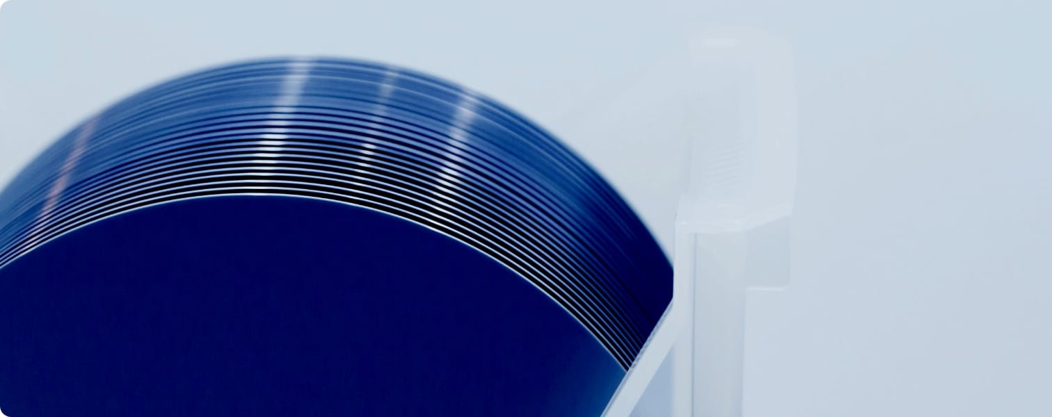
About the WM Series
The WM Series is an inspection system designed to detect particles and other defects on non-patterned wafer surfaces.
As an industry-standard tool for process and equipment management, it is widely used for various applications.
The system also supports a wide range of wafer sizes, offering high versatility as a key feature.
Applications
- System Control
- Process control
- Material & component management
- Equipment pre-shipment inspection
- R&D
- Wafer in-process & pre-shipment inspection, and more.
Target Markets
- Device manufacturers
- R&D
- Material mfrs.
- Chemical material manufacturers
- Equipment manufacturers
- Silicon and compound wafer manufacturers , and more.
Particle Detection Examples
-
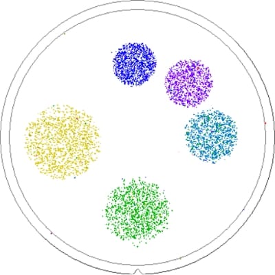
About PSL Calibration Wafer
-

High cost-performance
-

Compatible with
various wafer sizes -

Space-saving design
-

High sensitivity and wide dynamic range
Specifications
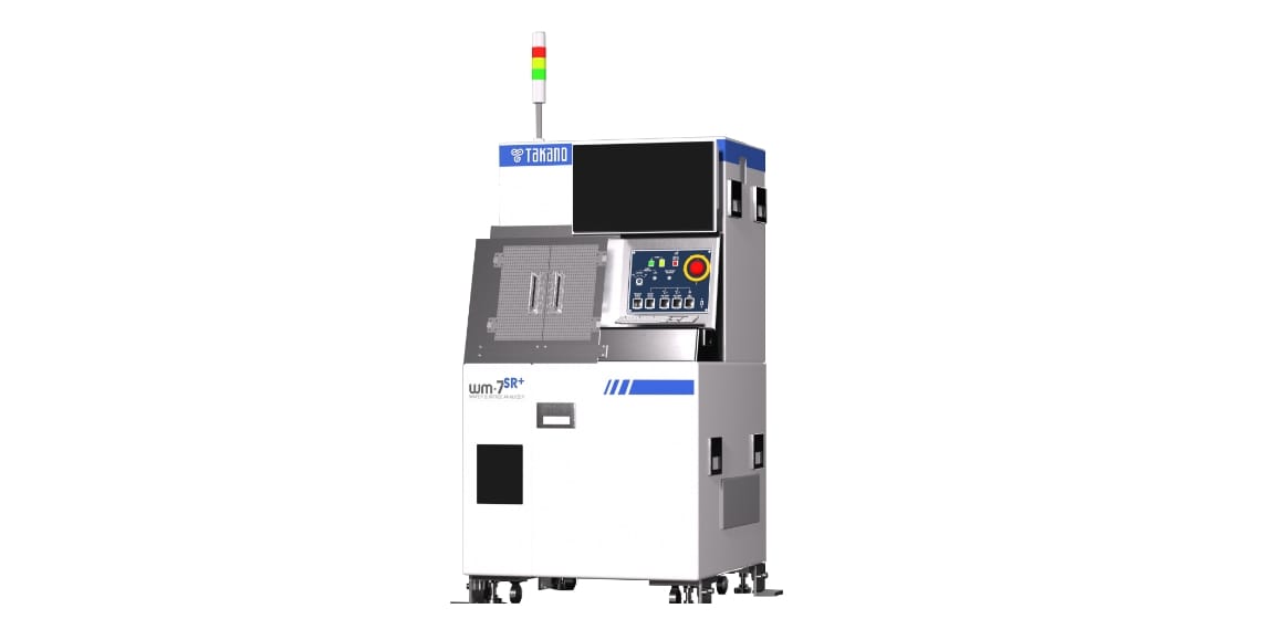
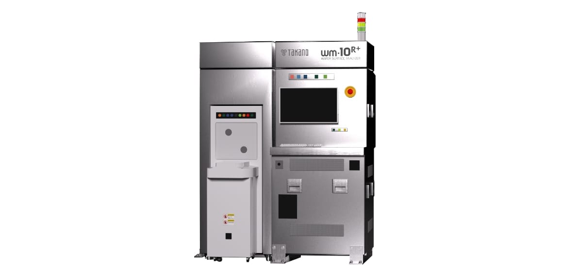
| Main Specifications | WM-7SR+ | WM-10R+ |
|---|---|---|
| Maximum Detection Sensitivity (Bare-Si) | 79nm (61nm optional) | 48nm |
| Wafer Size | 2–8inch | 4–12inch |
| Dynamic Range | 79nm to 5.0μm | 48nm to 5.0μm |
| System Size (mm) | W860 x D905 x H1655 | W1530 × D1242 × H1955 |
| International Certifications | SEMI, FDA, CE, UKCA | |