
Products Products
Semiconductor
WM, Vi, ALTAX, Thinspector, PSL
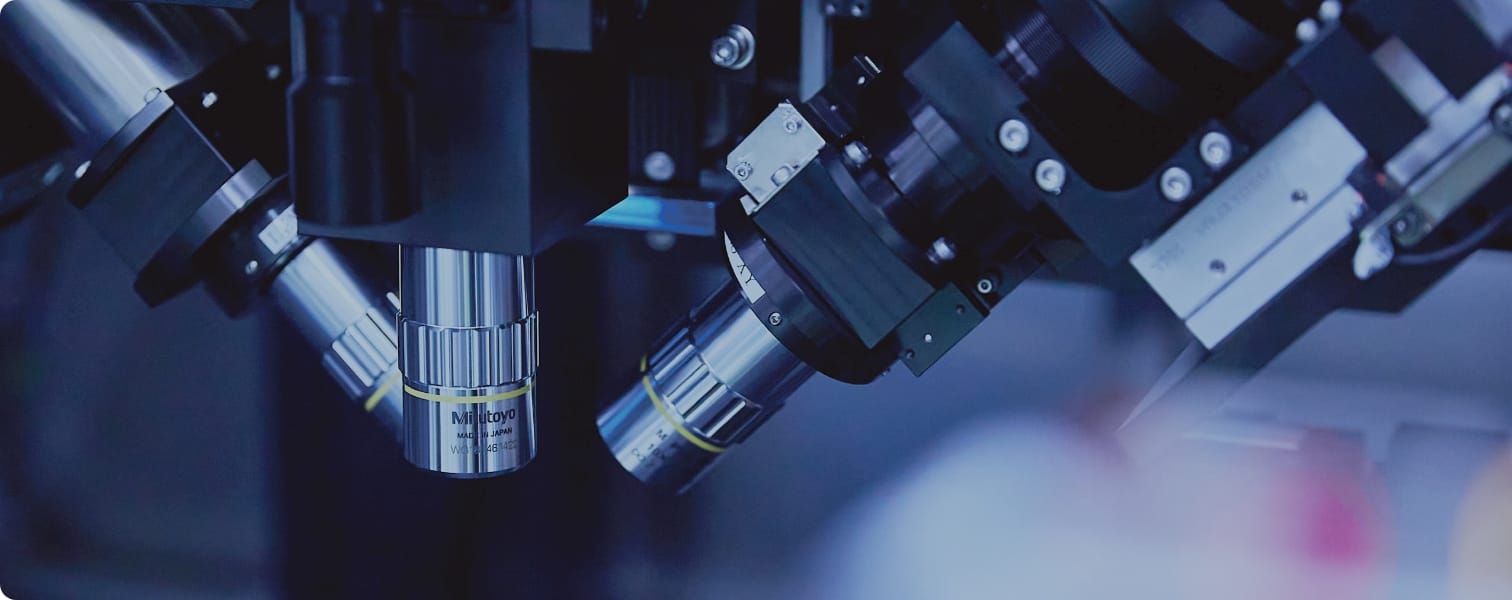
Through the development and manufacture of high-performance inspection systems, Takano supports the semiconductor industry with high-quality solutions.
Systems
-
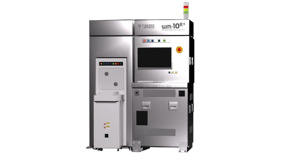
Front-End Inspection Systems
Takano inspection systems are optimal solution for front-end processes, tailored specifically for device manufacturing process. It supports process control inspections, foreign objects detection, particle inspection, and film thickness measurement.
-
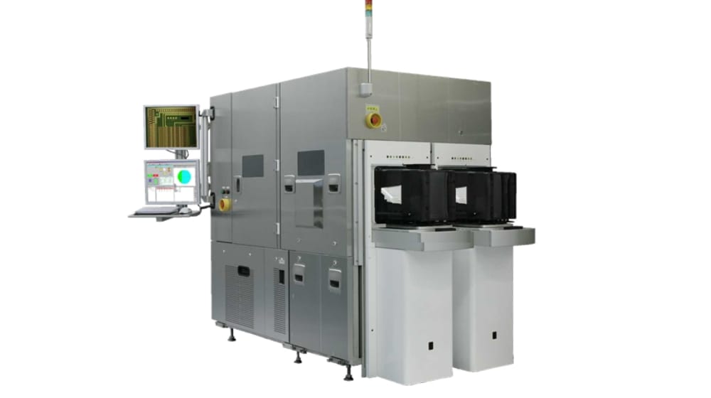
Back-End Inspection Systems
Takano supports various types of visual inspection systems used in post-dicing, post-expanding, and overall back-end processes, offering solutions tailored to meet each customer's specific needs
-
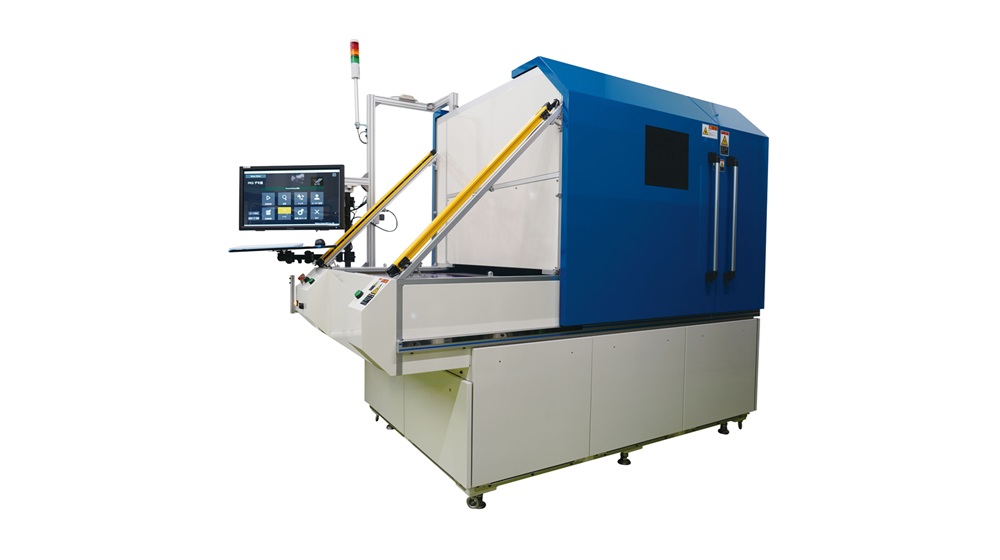
Packaging Inspection Systems
Dedicated inspection systems for wafer and substrate packaging.
Compatible not only with semiconductors but also with electronic components. -
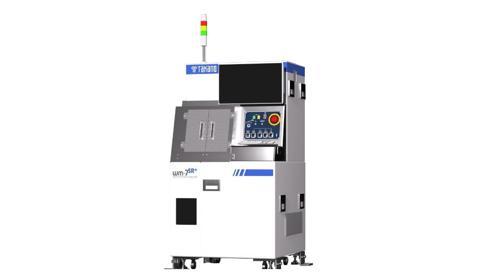
Inspection Systems for Material and Equipment Manufacturers
Optimal inspection systems for process control and outgoing quality control for substrate manufacture, such as compound semiconductors and process equipment manufactures.
About PSL Calibration Wafer
-

About PSL Calibration Wafer
Takano offers internationally certified Polystyrene Latex (PSL) sphere particle deposition services, fully traceable to NIST-USA standards.
Our advanced deposition system ensures precise, high-quality results on not only silicon (Si) wafers, but also a wide range of customer-supplied filmed wafers—perfect for system calibration, process optimization, and equipment quality control.
Film
HAWKEYES Series
As functionality and quality continue to evolve across industries, the demand for more advanced capabilities in Roll-to-Roll processes increases. HAWKEYES enables high-speed inspection of minute, low-contrast, and scratch defects, addressing the needs of this increasingly sophisticated Roll-to-Roll production process.
Ultra High-Speed Plain Film Inspection System
-
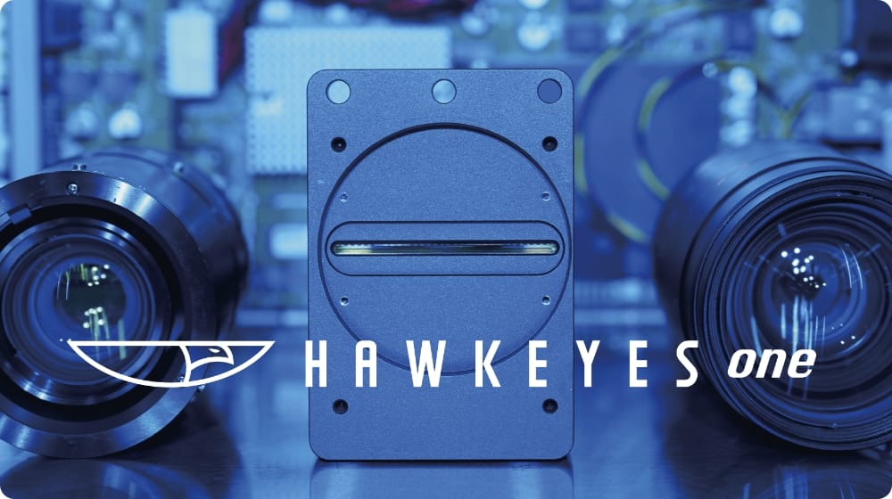
HAWKEYES ONE
An industry-leading inspection system that supports ultra-fast production lines! HAWKEYES ONE detects and classifies fine defects in real-time, significantly reducing the risk of defects escaping. Enhance quality control while boosting production efficiency!
Plain Film Inspection System
-
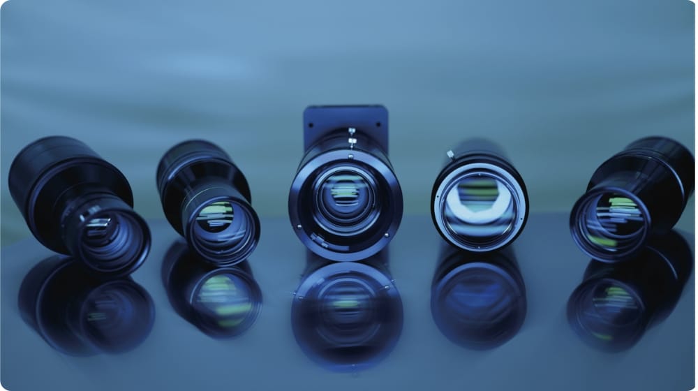
HAWKEYES ELITE
Combining high-speed, high-definition inspection with unmatched customizability, delivering flexible solutions that adapt to your unique needs and drive greater productivity.
Patterned Film Inspection System
-
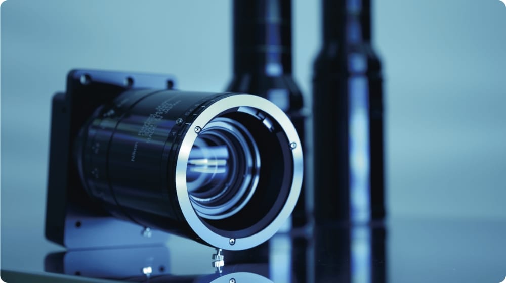
HAWKEYES PATTERN
Inspects patterned films in the Roll-to-Roll process with unique algorithms and advanced image processing hardware.
FPD
AOI & Mura
Supporting the production of LCD TVs, smartphones, and other various flat-panel displays, Takano create inspection and measurement equipment that drives quality improvements in manufacturing.
High-Precision Inspection System
-
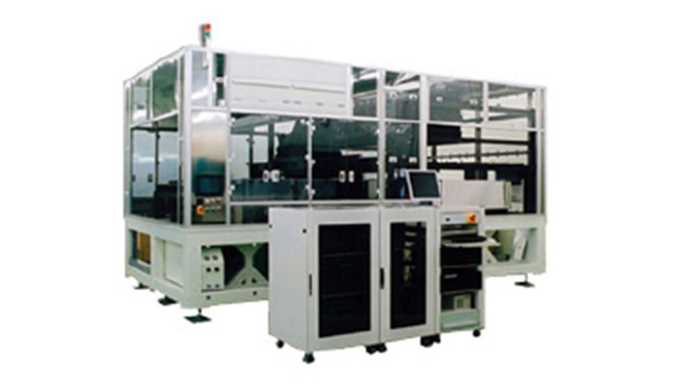
AOI
High-resolution inspection systems compatible with increasingly high-definition LCDs, OLEDs, and touch panel substrates.
Mura/Film Thickness Inspection System
-
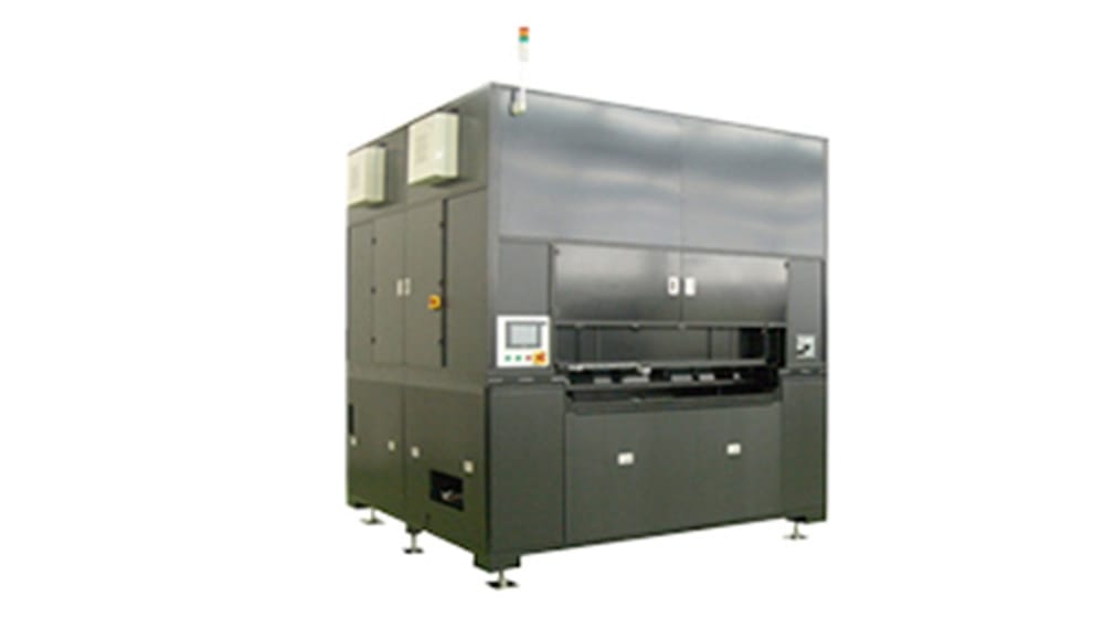
Mura
Effortlessly detect and eliminate mura (unevenness) defects in the FPD production process, reducing defects, minimizing losses, and driving significant improvements in yield.
Glass Substrate for AP
Vi, ALTAX, Thinspector
Inspection systems using the latest technology, compatible with transparent substrates.
We provide high-precision solutions for various applications, especially dent inspection after TGV hole filling or plating.
Patterned Wafer Visual Macro Inspection System
-
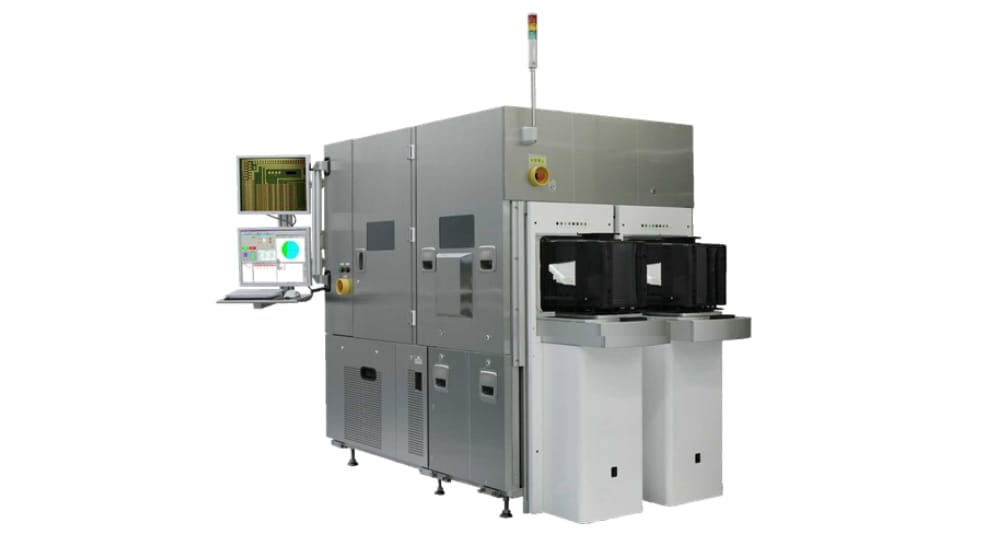
Vi Series
Vi Series performs high-speed, high-precision macro defect inspection of circuit patterns, color variations, and cracks.
With full compatibility for transparent wafers, it offers a versatile and powerful solution for a wide range of applications, ensuring unmatched quality and reliability.
Bump Height Inspection System
-
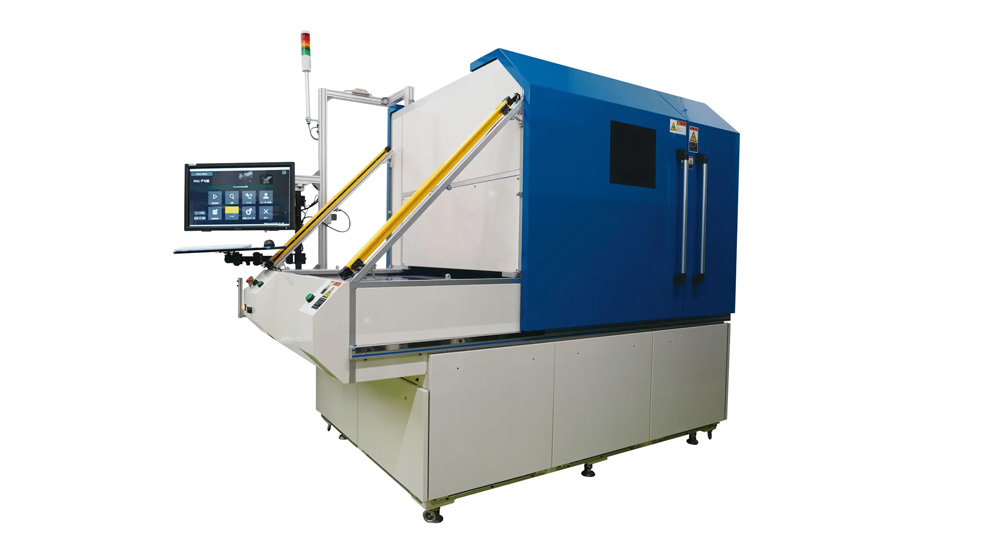
ALTAX Series
ALTAX Series performs high-speed, high-resolution measurement of bump height, diameter, and coplanarity on semiconductor wafers and package substrates such as BGA and CSP, also support dent inspection after via filling and plating. Improved optics and data processing enable higher accuracy than conventional light-section method.
Whole-Surface Film Thickness Inspection System
-
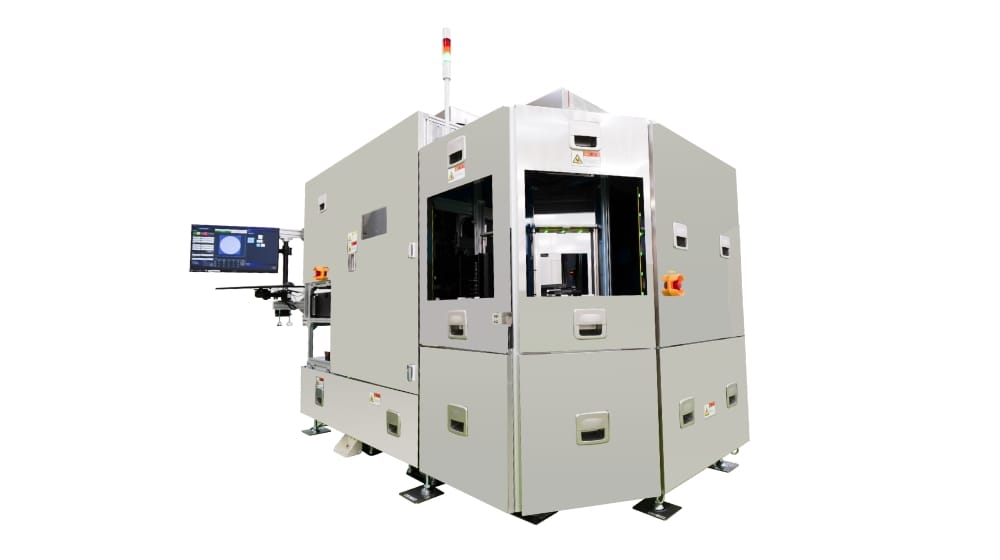
Whole-Surface Film Thickness Inspection System (Thinspector)
Thinspector enables inspection of non-uniformity or film thickness across the entire wafer surface in a single scan.